Research in Yang's group
-We bring unparalleled impacts to the fields we are involved in-
Our research involves advanced technologies in thin film solar cells, transparent conductors, metal oxide transistors, and other electronic devices. We have applied various kinds of semiconductor materials including conjugated polymers and organic molecules, carbon-based nanomaterials (CNT and graphene), hybrid semiconductors such as perovskite, and inorganic semiconductors (CZTS, CIGS) to pursue high performance thin film devices, such as LED, solar cell, transistor and digital memory. Our research strategy is primarily on the design/synthesis of solution-processable materials; understanding basic materials properties; forming unique (or novel) devices and investigating the physical properties of device physics.
Our exciting research topics have significantly impacted the field and have provided large potential for future applications. For example, since 2005, our organic and polymer PV research has ranked highly in both efficiency and fundamental research impact. Our publication titled High-efficiency solution processable polymer photovoltaic cells by self-organization of polymer blends has been cited more than 3500 times since 2005 (Nature Materials, 4, 864, 2005).
Due to his highly active research, Prof. Yang has been recognized by Thomas Reuters as one of the top-10 highly cited scientists from 2009-2010. In addition, he has received distinct recognition as a Highly Cited Researcher in Chemistry and Materials Science (2014), a survey conducted every 10 years to recognize highly versatile researchers in multiple fields. Recently, he has become the Fellow of Royal Society of Chemistry (FRSC), SPIE, and the Electromagnetic Academy, respectively. The details of our research are described below.
Organic Photovoltaics (OPV): This important research effort was launched in 2002. Our emphasis is on novel polymer design and synthesis, the understanding and control of device morphology, and the engineering of interface between inorganic/organic, and organic/organic materials. All of these efforts have lead to achieving higher device performances and have set the benchmarks for this field. During 2007 - 2011, we have achieved three world records on single junction solar cells (some of them through working with Solarmer Energy Inc). This record was recently replaced by our double-junction tandem solar cell devices with 10.6% efficiency (Nat. Comm., 4, 1446, 2013) and further enhanced to 11.6% efficiency by triple-junction tandem solar cells (Adv. Mat., 26, 5670, 2014). Two newly emerged sub-directions of OPV research include (1) transparent OPV (TOPV) and (2) small molecule OPV devices. In 2013, we utilized infrared absorbing polymers in a tandem design to demonstrate transparent tandem solar cells with 7% conversion efficiency. (Energy and Environmental Sci., 6, 2714, 2013). Similarly, in 2013 our OPV devices based on small molecules reached efficiencies surpassing 10% (Adv. Mat. 25, 4657, 2013). Both of these examples hold the best records in their fields, respectively.
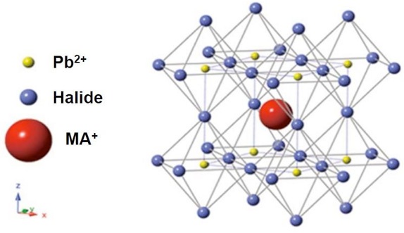
Hybrid Lead Halide Perovskite Solar Cells: This is an entirely new direction initiated in late 2012. In general, perovskite materials follow the formula ABX3 and adopt the same crystal structure as calcium titanate. In this arrangement, the A and B cations coordinate with 12 and 6 X anions, forming cuboctahedral and octahedral geometries, respectively (Figure 1).

Figure 1: Crystal lattice of the methylammonium lead halide (CH3NH3PbX3) perovskite structure.
The perovskite family exhibits a wide range of electronic behavior including piezoelectric, thermoelectric, semiconducting, and superconducting properties depending on the respective atoms within the crystal structure. In our research, the perovskite material is based on the compound CH3NH3PbX3 (X=Cl, Br, I), see Figure 1. Our accumulated experience with inorganic CIGS and OPV has provided a large advantage for expansion of perovskite research, allowing a rapid increase in efficiency from 1% in May of 2013 to near 20% in May of 2014. Within a year, we have published three important manuscripts on crystal growth mechanisms (JACS, 136, 622, 2014), flexible solar cells (ACS Nano, 8, 1674, 2014), and interface engineering, respectively (Science, 345, 542, 2014). We anticipate this research will soon exceed the 20% efficiency barrier.
Solution-processable Cu-Zn-Sn-S (or Se) (CZTS) semiconductors: Recently, CZTS solar cells have attracted significant attention in an effort to replace indium, an expensive rare earth metal in the technologically successful CIGS, with earth abundant zinc and tin. Through a novel design of nano-crystals, we have gained significant control to reach the desired phase of CZTS (Energy and Environment Science, 998, 2014) Subsequently, another approach is to use hydrazine as the solvent, thus allowing the CZTS precursor to be dissolved directly. By adding dry-ice (solid CO2) into the precursor solution, we were able to obtain a homogenous solution with excellent film quality (Adv. Mat., 24, 6323, 2012). The CZTS research involves significant material research in the solid-solvent reaction, and the formation of a compound semiconductor. The phase diagram in these compounds has not been entirely explored, thus further fundamental research is still of interest.
Metal-oxide Transistors and Electronics: Our group has extensive experience with transistors dating back to the days of the vertical transistor (2004-2009). Since 2013, we began to develop soluble metal oxide thin film transistors based on soluble inorganic semiconductor bases with intentions of replacing Si-based transistor backpanes in displays. Our research focuses on solution processable double layer In-Ga-Zn-Oxide (IGZO) transistors, demonstrating high carrier mobilities up to 40cm2/Vs within just 1.5 years of investigation (Adv. Mat., 26, 4273, 2014). In an effort to develop a lithography-free process, we have also demonstrated a low-temperature, self-patterning process. (ACS Nano, 8, 9680, 2014) Currently, this research is moving at a rapid pace and we hope someday this technology can be applied in the next generation wall-size display, where the displays will be printed directly.